Samsung Foundry

Samsung Foundry is set to detail its second generation 3 nm-class fabrication technology as well as its performance-enhanced 4 nm-class manufacturing process at the upcoming upcoming 2023 Symposium on VLSI Technology and Circuits in Kyoto, Japan. Both technologies are important for the contract maker of chips as SF3 (3GAP) promises to offer tangible improvements for mobile and SoCs, whereas SF4X (N4HPC) is designed specifically for the most demanding high-performance computing (HPC) applications. 2nd Generation 3 nm Node with GAA Transistors Samsung's upcoming SF3 (3GAP) process technology is an enhanced version of the company's SF3E (3GAE) fabrication process, and relies on its second-generation gate-all-around transistors – which the company calls Multi-Bridge-Channel field-effect transistors (MBCFETs). The node promises additional process optimizations, though the foundry prefers not to compare...
Inflation Drives Up Fab Costs for Intel and Samsung by Billions of Dollars
To address future demand for semiconductors amid severe chip shortages of 2020 – 2022, all leading chipmakers announced plans to build new fabs and even disclosed their estimated costs...
15 by Anton Shilov on 3/16/2023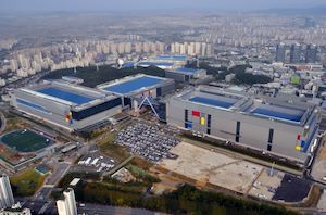
Samsung Seeks to Make South Korea No. 1 Chipmaker with $230B Investment Over 20 Years
Samsung on Wednesday unveiled their plan to invest $230 billion over the next 20 years in a new semiconductor production mega cluster in South Korea. The country's government believes...
22 by Anton Shilov on 3/15/2023
Samsung's $15 Billion R&D Complex to Overcome Limits of Semiconductor Scaling
Samsung on Friday broke ground for a new semiconductor research and development complex which will design new fabrication processes for memory and logic, as well as conduct fundamental research...
26 by Anton Shilov on 8/19/2022
Samsung Starts 3nm Production: The Gate-All-Around (GAAFET) Era Begins
Capping off a multi-year development process, Samsung’s foundry group sends word this morning that the company has officially kicked off production on its initial 3nm chip production line. Samsung’s...
22 by Ryan Smith on 6/30/2022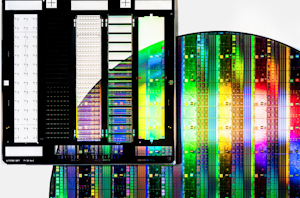
ASML High-NA Development Update: Coming to Fabs in 2024 - 2025
It took the semiconductor industry over a decade to prep everything needed for production of chips using extreme ultraviolet (EUV) lithography. It looks like it is going to take...
8 by Anton Shilov on 5/26/2022
Applied Materials Outlines Next-Gen Tools for 3nm and GAA Transistor Era
Last month Samsung Foundry quietly announced that it was set to begin producing chips using its 3GAE (3 nm-class, gate-all-around transistors, early) process technology in the second quarter. While...
17 by Anton Shilov on 5/12/2022Universal Chiplet Interconnect Express (UCIe) Announced: Setting Standards For The Chiplet Ecosystem
If there has been one prominent, industry-wide trend in chip design over the past half-decade or so, it has been the growing use of chiplets. The tiny dies have...
25 by Ryan Smith on 3/2/2022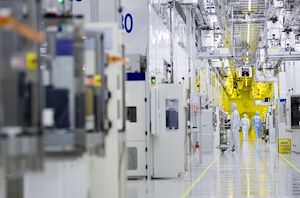
Semi CapEx to Hit $152 Billion in 2021 as Market on Track for $2 Trillion by 2035
Semiconductor makers have drastically increased their capital expenditures (CapEx) this year in response to unprecedented demand for chips that is going to last for years. Now the CEO of...
8 by Anton Shilov on 12/17/2021
Texas To Get Multiple New Fabs as Samsung and TI to Spend $47 Billion on New Facilities
After a year of searching for the right place of its new U.S. fab, Samsung this week announced that it would build a fab near Taylor, Texas. The company...
135 by Anton Shilov on 11/24/2021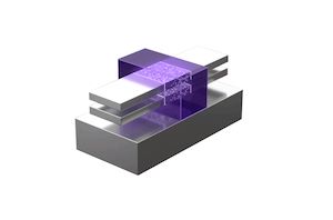
Samsung Foundry: 2nm Silicon in 2025
One of the key semiconductor technologies beyond 3D FinFET transistors are Gate-All-Around transistors, which show promise to help extend the ability to drive processors and components to higher performance...
29 by Dr. Ian Cutress on 10/6/2021
Samsung Foundry’s New 17nm Node: 17LPV brings FinFET to 28nm
Despite most discussion about chip manufacturing focusing on the leading edge and blazingly fast and complex side of the industry, the demand for the ‘legacy’ process technologies is also...
11 by Dr. Ian Cutress on 10/6/2021
Samsung Foundry to Almost Double Output by 2026
It’s hard not to notice that we’re in the middle of a semiconductor crunch right now. Factories are running at full steam, but pinch points in the supply chain...
6 by Dr. Ian Cutress on 10/6/2021
Samsung: Deployment of 3nm GAE Node on Track for 2022
Samsung Foundry has made some changes to its plans concerning its 3 nm-class process technologies that use gate-all-around (GAA) transistors, or what Samsung calls its multi-bridge channel field-effect transistors...
32 by Anton Shilov on 7/9/2021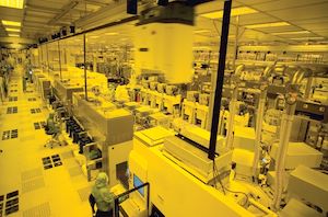
Sales of Fab Tools Surge to Over $71 Billion in 2020
SEMI, an organization representing chipmakers and producers of semiconductor production tools, published this week that sales of wafer processing equipment has surged to an all-time record of $71.19 billion...
18 by Anton Shilov on 4/15/2021
EUV Pellicles Ready For Fabs, Expected to Boost Chip Yields and Sizes
Foundries started limited usage of extreme ultraviolet (EUV) lithography for high-volume manufacturing (HVM) of chips in 2019. At the time, ASML's Twinscan NXE scanners were good enough for production...
35 by Anton Shilov on 3/31/2021
Report: Semi Demand 30% Above Supply, 20% Year-on-Year Growth
Semiconductor foundry offerings are thriving due to unprecedented demand for semiconductors and processors in recent quarters. Analysts from TrendForce believe that in Q1 2021 foundries will increase their revenue...
31 by Anton Shilov on 2/25/2021
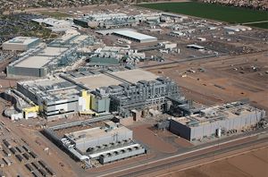
Samsung Foundry: New $17 Billion Fab in the USA by Late 2023
Samsung Foundry has filed documents with authorities in Arizona, New York, and Texas seeking to build a leading-edge semiconductor manufacturing facility in the USA. The potential fab near Austin...
36 by Anton Shilov on 2/10/2021
Samsung Announces "X-Cube" 3D TSV SRAM-Logic Die Stacking Technology
Yesterday, Samsung Electronics had announced a new 3D IC packaging technology called eXtended-Cube, or “X-Cube”, allowing chip-stacking of SRAM dies on top of a base logic die through TSVs. Current...
21 by Andrei Frumusanu on 8/14/2020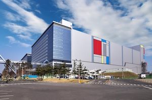
Samsung Starts Mass Production at V1: A Dedicated EUV Fab for 7nm, 6nm, 5nm, 4nm, 3nm Nodes
Samsung Foundry has started mass production of chips using its 6LPP and 7LPP manufacturing processes at its new V1 fab. The new facility employs one of the industry’s first...
30 by Anton Shilov on 2/20/2020


