4nm

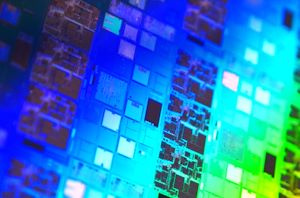
Samsung Foundry is set to detail its second generation 3 nm-class fabrication technology as well as its performance-enhanced 4 nm-class manufacturing process at the upcoming upcoming 2023 Symposium on VLSI Technology and Circuits in Kyoto, Japan. Both technologies are important for the contract maker of chips as SF3 (3GAP) promises to offer tangible improvements for mobile and SoCs, whereas SF4X (N4HPC) is designed specifically for the most demanding high-performance computing (HPC) applications. 2nd Generation 3 nm Node with GAA Transistors Samsung's upcoming SF3 (3GAP) process technology is an enhanced version of the company's SF3E (3GAE) fabrication process, and relies on its second-generation gate-all-around transistors – which the company calls Multi-Bridge-Channel field-effect transistors (MBCFETs). The node promises additional process optimizations, though the foundry prefers not to compare...
Samsung Foundry Vows to Surpass TSMC Within Five Years
The head of Samsung's semiconductor unit acknowledged last week that the company's current mass production, leading-edge process technologies are a couple of years behind TSMC's most advanced production nodes...
12 by Anton Shilov 4 days ago
TSMC Announces Early Access Nodes for Next-Gen Car Chips: N4AE and N3AE
As the final set of announcements from this week's North American Technology Symposium, TSMC closed out their fab roadmap updates with some fresh news on their automotive-centric processes. For...
10 by Anton Shilov on 4/28/2023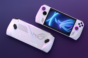
Asus Preps ROG Ally: A Portable Windows Game Console with Custom Zen 4 + RDNA 3 APU
Asus has begun teasing its own portable game console, the ROG Ally, which the company is positioning as a high-end offering for the handheld PC gaming market. With its...
18 by Anton Shilov on 4/5/2023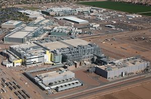
Inflation Drives Up Fab Costs for Intel and Samsung by Billions of Dollars
To address future demand for semiconductors amid severe chip shortages of 2020 – 2022, all leading chipmakers announced plans to build new fabs and even disclosed their estimated costs...
15 by Anton Shilov on 3/16/2023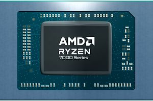
AMD Lays Out 2023 Ryzen Mobile 7000 CPUs: Top-to-Bottom Updates, New Zen 4 'Phoenix' CPU Takes Point
This year’s CES has turned out to be a laptop-centric event in the PC space, and no farther do you have to look for proof of that than AMD’s...
46 by Ryan Smith on 1/4/2023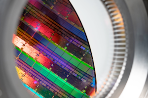
TSMC and ASML: Demand for Chips Remains Strong, But Getting Fab Tools Is Hard
TSMC's revenue this year is going to set an all-time record for the company, thanks to high demand for chips as well as increased prices that its customers are...
13 by Anton Shilov on 7/21/2022
AMD: We’re Using an Optimized TSMC 5nm Process
When AMD started using TSMC’s 7nm process for the Zen 2 processor family that launched in November 2019, one of the overriding messages of that launch was that it...
44 by Dr. Ian Cutress on 1/10/2022
TSMC Unveils N4X Node: Extreme High-Performance at High Voltages
TSMC this week announced a new fabrication process that is tailored specifically for high-performance computing (HPC) products. N4X promises to combine transistor density and design rules of TSMC's N5-family...
42 by Anton Shilov on 12/17/2021
TSMC Roadmap Update: 3nm in Q1 2023, 3nm Enhanced in 2024, 2nm in 2025
TSMC has introduced a brand-new manufacturing technology roughly every two years over the past decade. Yet as the complexity of developing new fabrication processes is compounding, it is getting...
32 by Anton Shilov on 10/18/2021
Samsung: Deployment of 3nm GAE Node on Track for 2022
Samsung Foundry has made some changes to its plans concerning its 3 nm-class process technologies that use gate-all-around (GAA) transistors, or what Samsung calls its multi-bridge channel field-effect transistors...
32 by Anton Shilov on 7/9/2021
TSMC Update: 2nm in Development, 3nm and 4nm on Track for 2022
For TSMC, being the world's largest foundry with nearly 500 customers has its peculiarities. On the one hand, the company can serve almost any client with almost any requirements...
74 by Anton Shilov on 4/26/2021
Samsung Starts Mass Production at V1: A Dedicated EUV Fab for 7nm, 6nm, 5nm, 4nm, 3nm Nodes
Samsung Foundry has started mass production of chips using its 6LPP and 7LPP manufacturing processes at its new V1 fab. The new facility employs one of the industry’s first...
30 by Anton Shilov on 2/20/2020
Samsung’s Aggressive EUV Plans: 6nm Production in H2, 5nm & 4nm On Track
Samsung Foundry formally started to produce chips using its 7LPP (7 nm low power plus) fabrication process last October and has not slowdown development of its manufacturing technologies since...
42 by Anton Shilov on 7/31/2019
Synopsys to Accelerate Samsung’s 7nm Ramp with Yield Explorer Platform
Synopsys has announced an acceleration of development on its yield learning platform designed to speed up ramp up of chips made using Samsung Foundry’s 7LPP (7 nm low power...
16 by Anton Shilov on 7/4/2019
Samsung Foundry Updates: 8LPU Added, EUVL on Track for HVM in 2019
Samsung recently hosted its Samsung Foundry Forum 2018 in Japan, where it made several significant foundry announcements. Besides reiterating plans to start high-volume manufacturing (HVM) using extreme ultraviolet lithography...
29 by Anton Shilov on 9/6/2018


